1. Absorption of light in silicon
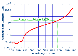 Absorption coefficient (intensity, not amplitude) of light in pure silicon.
Under most conditions, an absorbed photon results in an electron-hole pair,
one of which is detected. Note that the absorption length changes by nearly
four orders of magnitude over the interesting optical range.
Absorption coefficient (intensity, not amplitude) of light in pure silicon.
Under most conditions, an absorbed photon results in an electron-hole pair,
one of which is detected. Note that the absorption length changes by nearly
four orders of magnitude over the interesting optical range.
This is for room temperature, where the bandgap is at 1103 nm (1.125 eV). At -110 C the bandgap is at 1075 nm (1.154 eV).
Full size postscript version, (48616 bytes)
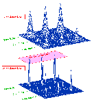
 Conventional front-illuminated and thinned scientific CCDs.
 The Berkeley Lab proposal: Use a high-resistivity (~10 kohm-cm) n-type
substrate, and operate fully depleted. A conductive rear window (ITO with
a possible SiO_2 coating) serves as rear contact and an antireflective
window.
The Berkeley Lab proposal: Use a high-resistivity (~10 kohm-cm) n-type
substrate, and operate fully depleted. A conductive rear window (ITO with
a possible SiO_2 coating) serves as rear contact and an antireflective
window.
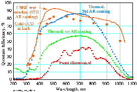 Quantum efficiency (QE) of the LBL/Lick CCd as compared with standard front-illuminated,
thinned back-illuminated, and thinned back-illuminated antireflective coated
CCDs. (The latter are from M. Blouke and M. Nelson, SPIE 1900, 228-240
(1993).
Quantum efficiency (QE) of the LBL/Lick CCd as compared with standard front-illuminated,
thinned back-illuminated, and thinned back-illuminated antireflective coated
CCDs. (The latter are from M. Blouke and M. Nelson, SPIE 1900, 228-240
(1993).